Ultra Low Noise Transistor Modeling
When modeling transistors for use in low noise amplifiers, special care must be taken to accurately simulate small signal noise performance. As the minimum achievable noise temperature drops, measurement uncertainty increases. This work documents the development of models for the OMMIC 4F200, a 70 nm GaAs pHEMT, and the Diramics 4F250, a 100 nm InP HEMT. A two step procedure was taken to completely extract the small signal and noise parameters with reasonable certainty using a modified Pospieszalski model.
Background
Small Signal Model
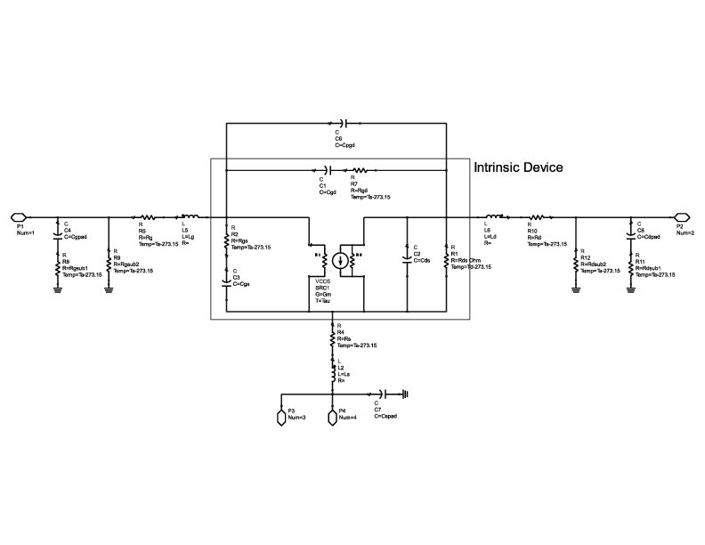
The small signal model of a HEMT (High Electron Mobility Transistor) is an expansion of the classic hybrid-pi model of a field effect transistor. There are two major sections of the model, the intrinsic and extrinsic regions. The intrinsic region represents the bias-dependent response of the transistor while the extrinsic region models the parasitics of the package. There are many variations of the model, some more accurate than others, but we kept with the popular 22 parameter model included as a starting point in the Diramics data sheet.
Noise Parameters
The four parameter noise model is the traditional method of expressing noise in a two port network with N, Tmin, Ropt, and Xopt. N describes the relationship between source match and noise, Tmin is the minimum achievable noise temperature, and Zopt is the impedance presented to the input of the network that minimizes the noise. The input impedance Zopt = Ropt + jXopt. The four noise parameters are related to the total noise temperature of the network by
$$\begin{aligned} T = T_{min} +NT_0\frac{|Z_{s}-Z_{opt}|^2}{R_{s}R_{opt}} \end{aligned}$$As there are four unknown parameters, one solution is to present four different Zs to the device with a tuner and record the noise temperature at the output and solve for the unknowns. This method is error-prone as both the source reflection and noise temperature have to be accurately measured, a difficult task with ultra low noise devices.
Equivalent HEMT Thermal Model
Traditionally, a noiseless two port network is cascaded with noise generators derived from the noise parameters. This requires a source-pull to extract noise parameters then a separate extraction of the small signal model parameters. While the noise parameter model describes any two port network, a simplification can be made for HEMTs. Noise performance can be simulated using only the noise contribution of the resistive elements in the small signal model. All resistors generate thermal noise following the Johnson–Nyquist formula
$$\begin{aligned} V_{Noise_{rms}} = \sqrt{4k_bTR\Delta{f}} \end{aligned}$$The driving variable in Pospieszalski's model is the temperature of the drain to source resistance, TDrain. While all other resistances are at the temperature of the test fixture, TDrain is on the order of 2000 K at room temperature. After parameter extraction of the small signal model, all that is required is one noise measurement to find TDrain. This method is preferred as it only requires one measurement with 50 Ω terminations that can be fitted to the model with only one variable. Also, the test setup does not need to be greatly modified from an S-Parameter setup used in the extraction of the 22 small signal parameters. This model is beneficial as the noise performance of the transistor is encapsulated in the small signal model. Noise contribution in the device is then directly associated with its physical characteristics, allowing for a more complete understanding.
A modification of this small signal noise model was made to include the effects of gate current. High gate current devices, like the OMMIC 4F200, have been found to introduce additional noise beyond the contribution of the thermal effects of the resistances and the channel noise. Two currents were measured and included in the model as shot noise using the Schottky formula
$$\begin{aligned} I_{Noise_{rms}} = \sqrt{2q_ei_{dc}\Delta{f}} \end{aligned}$$This was done to correctly model Γopt and Fmin of the device. Without compensation for gate current, TDrain would optimize higher and the subsequent noise parameters would be off. The complete small signal noise model is shown below
Extraction Methodology and Implementation
There are many different approaches to extracting the 22 elements of the small signal model. The most straightforward was a curve-fit approach with multiple biases. The procedure was to probe the die at different biases and save the S-Parameters. Then at the bias of interest, measure the noise temperature. As the noise source and noise figure analyzer are both matched to 50 Ω, this measurement parallels the noise figure simulation of just the transistor. Again at the bias of interest, the gate current was noted from the power supply. This measurement represents the total gate current. Changing VDS to match VGS eliminated gate to drain current and allowed for a readout of gate to source current. Simply subtracting IGS from IGTotal yields IGD.
Measurement Specifics
When probing for S-Parameters, the Agilent N5242A PNA-X was utilized. Measurements were taken from 10 MHz to 10 GHz. Probe calibration was performed to shift the reference plane to the edge of the die. Bias was brought in using the internal bias tees in the PNA-X. The Agilent N8975A NFA was used with an N4000A noise source to measure noise temperature. The N4000A noise source was calibrated against an LN_2 noise standard from 10 MHz to 2.5 GHz by S. Weinreb. Mini-Circuits bias tees were used to introduce bias for this noise measurement. S-Parameters were measured of the bias tees and output cable to create an input and output loss compensation table for the NFA. Both the S-Parameters and noise measurements included 64 times averaging.
Small Signal Curve Fit Procedure
A workspace was setup in Keysight's ADS to perform the optimization between the measured S-Parameters and the 22 element model. A parameterized subcircuit was created for the FET and the optimizer was set up to minimize the difference between the measured and simulated data. As we had data at multiple bias points, each set of data for the same transistor shared global extrinsic parameters. This way, the optimizer had a reference as to what parameters are bias-dependent. Eight different bias points were used in the extraction of the parameters for the OMMIC and Diramics transistors. As this resulted in 176 variables to simultaneously optimize, a simulated annealing optimization algorithm was utilized to minimize computation time. Simulated annealing is a metaheuristic algorithm in which an approximate global optimum can be found in a large search-space. As the search for a discrete optimum would be futile on a 176-D surface, a probabilistic optimum would suffice as the computation time for a convergent solution would be monumental.
If the bias point of interest was included in the simulated annealing procedure, only slight adjustments to the intrinsic parameters were needed to reach a convergent solution. Focusing on the single bias point, a quasi-newton optimization was utilized to perfect the intrinsic parameters. Simulated annealing brought the device's model to an approximate optimum fit, but a gradient-descent will converge on the discrete optimum. The quasi-newton method uses an approximate 2^nd derivative to find gradient direction then follows traditional gradient descent optimization.
Noise Fit Procedure
Once the extrinsic and intrinsic parameters were identified, a simple linear fit relates TDrain to T50.
Error
Much of the challenge in this type of modeling is in the minimization of error. A paper by J. Saijets explores in detail the origin of error in model-fitting using S-Parameters. The most error-prone measurement is the extraction of input resistance. In this model, input resistance includes the summation of R_G, R_GS, and R_s. This uncertainty originates from the magnitude of input capacitance at low frequencies. Given our typical total input resistance of 1.5 Ω and input capacitance of 150 fF, relative error beneath 5 GHz is well over 300%. Output impedance error has similar behavior where resistance dominates at low frequencies. By measuring out to 10 GHz, we can reduce relative error to approximately 20% for both resistance and capacitance. Saijets has shown that transconductance and feedback capacitance can be extracted with minimal error, around 4-5%.
Noise error is more problematic as the measurement is very sensitive to radio frequency interference and calibration. Given our test setup and calibration, we predict an average T50 error of ±5 K.
Results
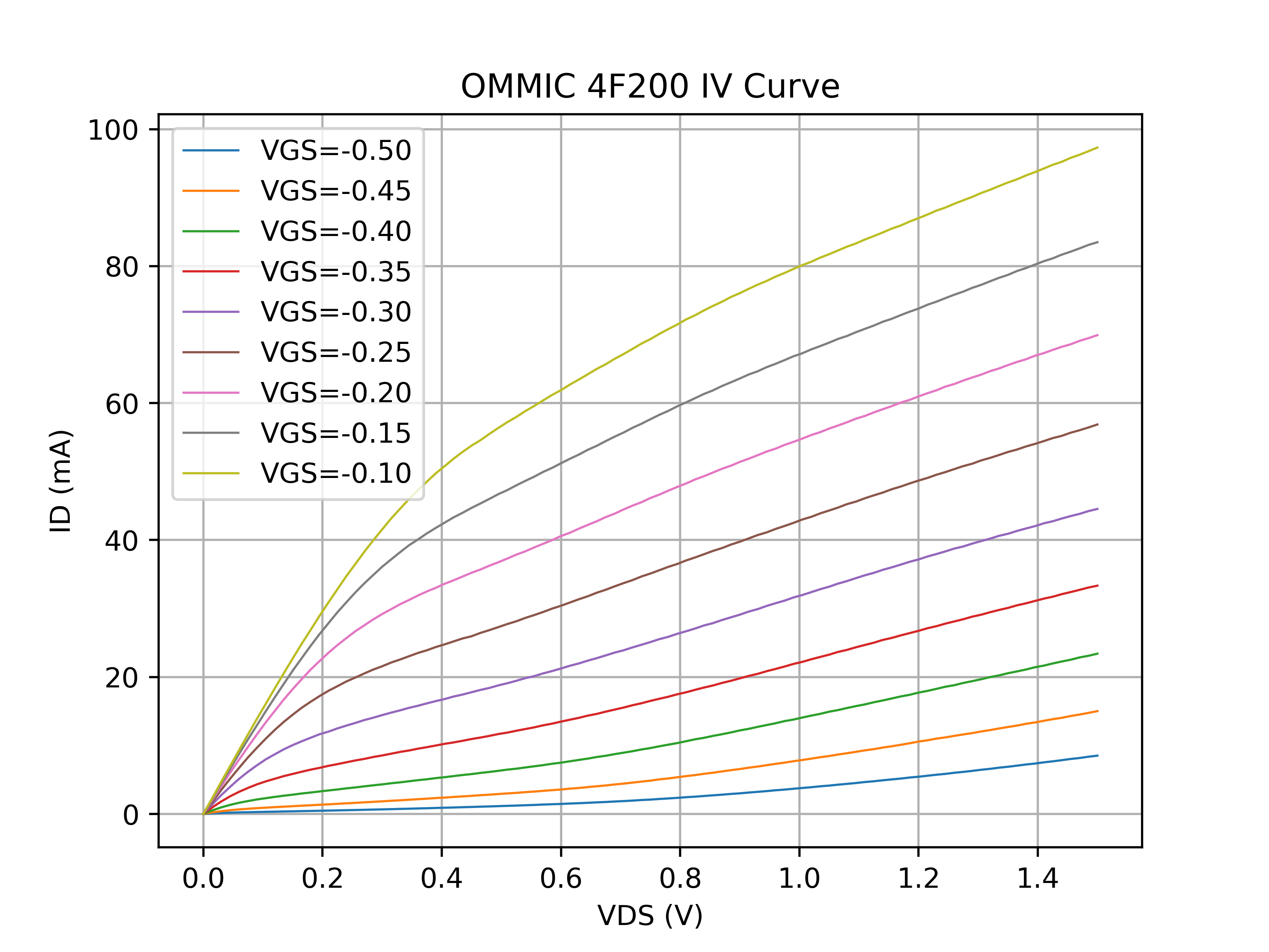
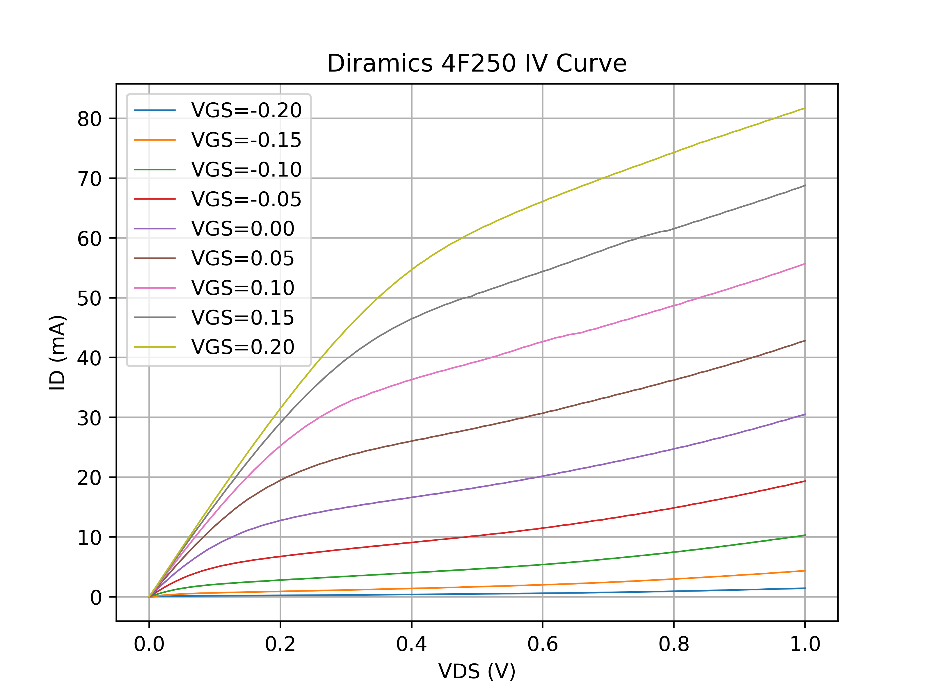
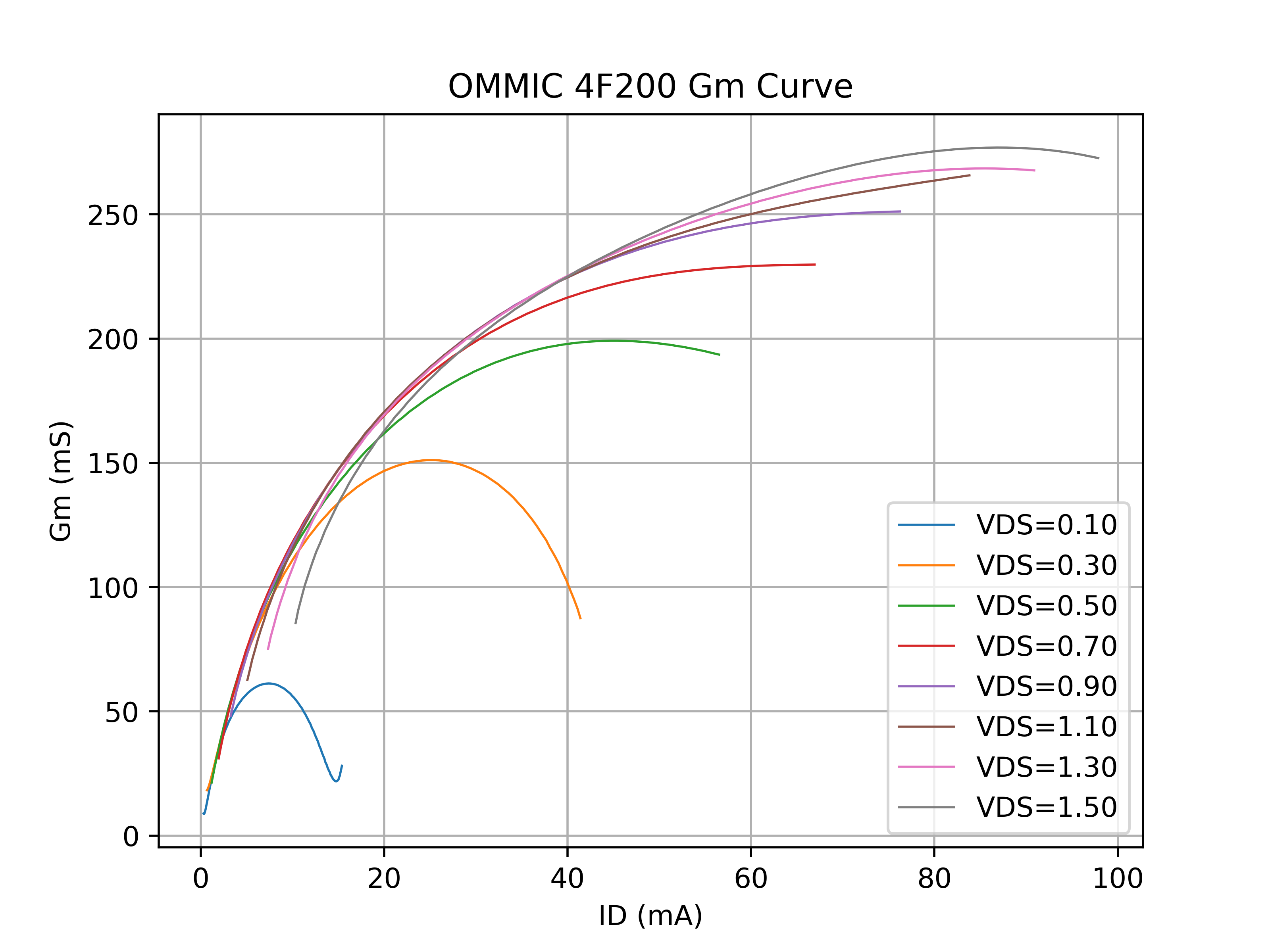
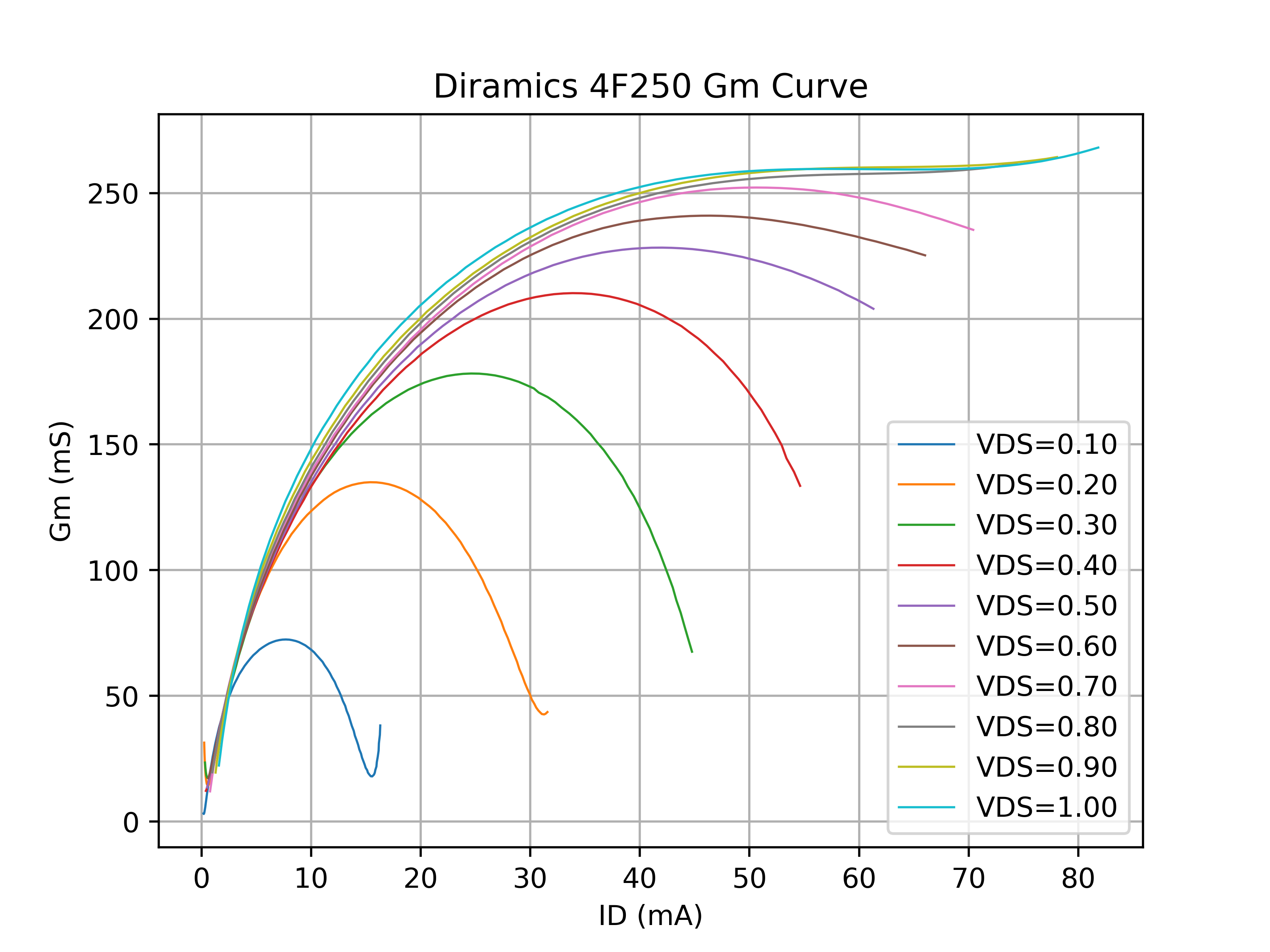
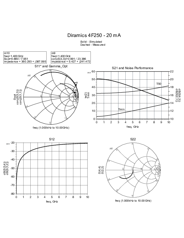
This work resulted in excellent agreement between measured and simulated data as shown in the plots below. T50 matches exactly what was measured with the NFA. Moving forward, validation of Γopt with a tuner could be used to further refine the model.

Appendix I - Extracted Parameters {#appendix-i-extracted-parameters}
| Diramics 4F250 | OMMIC 4F200 | |
|---|---|---|
| Rg ( Ω) | 0.53 | 1.57 |
| Rd (m Ω) | 560 | 471 |
| Rs (m Ω) | 913 | 411 |
| Lg (pH) | 45 | 70 |
| Ld (pH) | 43 | 65 |
| Ls (pH) | 2 | 2 |
| Rdsub1 ( Ω) | 62 | 75 |
| Rdsub2 (k Ω) | 427 | 200 |
| Rgsub1 ( Ω) | 55 | 27 |
| Rgsub2 (k Ω) | 196 | 200 |
| Cgpad (fF) | 5 | 15 |
| Cdpad (fF) | 4 | 36 |
| Cspad (fF) | 87 | 107 |
| Cpgdd (fF) | 2 | 0.7 |
| Diramics 4F250 | OMMIC 4F200 | |||||
|---|---|---|---|---|---|---|
| 40 mA/mm | 80 mA/mm | 160 mA/mm | 50 mA/mm | 150 mA/mm | 250 mA/mm | |
| Cgs (fF) | 133 | 144 | 163 | 95 | 106 | 108 |
| Cgd (fF) | 49 | 52 | 56 | 43 | 44 | 47 |
| Cds (fF) | 70 | 64 | 91 | 39 | 42 | 32 |
| Rgs (m Ω) | 700 | 692 | 2000 | 945 | 108 | 304 |
| Rgd ( Ω) | 4 | 1 | 2 | 2 | 3 | 0.45 |
| Rds ( Ω) | 70 | 39 | 23 | 62 | 32 | 22 |
| Gm (mS) | 151 | 259 | 367 | 120 | 224 | 285 |
| Tau (ps) | 0.163 | 0.171 | 0.150 | 0.178 | 0.159 | 0.165 |
| Td (K) | 2434 | 2944 | 3237 | 2129 | 3913 | 2723 |
| Igd (nA) | 3 | 3 | 3 | 1623 | 1254 | 960 |
| Igs (nA) | 0.1 | 0.1 | 0.1 | 47 | 316 | 190 |
| TMin (K) | 5 | 4 | 5 | 14 | 12 | 9 |
| T50 (K) | 40 | 33 | 32 | 61 | 62 | 44 |
| N | 0.021 | 0.015 | 0.017 | 0.03 | 0.029 | 0.02 |
| ROpt ( Ω) | 335 | 360 | 311 | 350 | 360 | 371 |
| XOpt ( Ω) | 404 | 387 | 307 | 186 | 232 | 206 |
Appendix II - DC Data {#appendix-ii-dc-data}