A 6x6 Aperture-Coupled Stacked Patch Phased Array for Wideband Ku Radar
In this post, the theory and design of a phased array for wideband Ku radar (12-18 GHz) operation using Ansys HFSS is presented. Starting with performance assumptions from the application specified, an aperture coupled stacked-patch arrangement is designed. A unit cell was then optimized for the required operation conditions. Once the unit cell was perfected, the array-factor driven rectangular array was created to understand gain performance. Finally, a full wave simulation was performed using finite array domain decomposition and finite-element boundary integrals on the USF CIRCE cluster. Performance of the phased array is then shown to meet the design requirements of 20dB gain broadside and steerable to over \(60^{\circ}\) in the X and Y plane.
Initial Design Considerations
The application of this antenna system is to be for Ku-Band radar. This section of spectrum (12-18 GHz) is an excellent candidate for both military and scientific endeavors. Specifically, it has been found that the Ku band is well suited for arctic radiometric and imagery applications as snow and ice react poorly to lower-frequency systems. As the Ku band is nearing millimeter wave, electronics and their associated systems decrease in size. This allows for easier integration into airborne and spaceborne systems where size and weight are large concerns. In regards to the array's radar application, if can be assumed that the system is frequency modulated continuous wave (FMCW), then a wideband chirp is highly desirable for increased range resolution.
$$\begin{aligned} \delta_r = \frac{c}{2B} \end{aligned}$$For compatibility with other systems, and to reap the benefits of the Ku band, the array will be made to cover the entire Ku band (12-18 GHz). Additionally, it would be extremely beneficial if this array was electrically steerable. The wider the scan angle, the larger the area the antenna can scan. Finally, if this were an airborne or spaceborne system, the distance from the array to the target could be very great. Having a high gain system paired with sensitive receivers is the optimum situation for good radar performance as the received signal needs to be large enough to be processed in context of the background noise. High gain is consequence of a purposefully fed and well laid out design as it is desirable to have minimum coupling between elements and low grating lobes.
To summarize the design requirements:
| Requirement | Specification |
|---|---|
| Bandwidth | 12-18 GHz |
| Gain | 20 dB |
| Scan Angle | Above \(60^{\circ}\) |
Unit Cell Theory
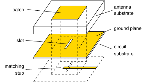
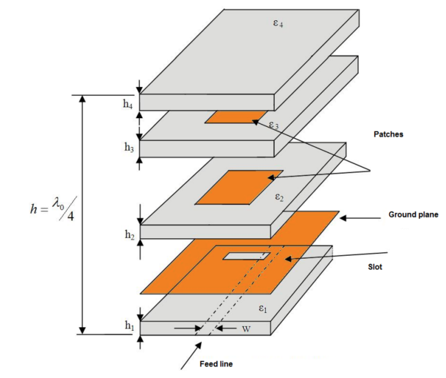
For a phased array to behave within specifications, the unit cell for the array must be well thought out. An element with too high gain won't have the capability to be steered as much as an omnidirectional design. An element that is electrically large won't be able to be cascaded in the array without grating lobes. Finally, the unit cell needs to be physically realizable. The first antenna under investigation for unit cell possibility is a standard microstrip fed patch antenna. This antenna, Fig. 1, is an incredibly simple design. A patch antenna is effectively a resonant structure fed into a point with an approximate input impedance of 50\(\Omega\). A patch antenna also has relatively high gain at around 7dB. The simple patch antenna almost meets the criteria for our radar except for a few shortcomings. It is well known that a patch antenna has a small bandwidth, on the order of 0.5-1%. Also, the approximate length of the path is \(\lambda/2\). If the radiating element is already large, any array with this cell will have grating lobes. So, a better design needs to be chosen. The second type of antenna under consideration is an aperture-coupled patch antenna, Fig. 2. This operates under the same principle of the inset fed path, except for the fact that the geometry is excited through an aperture instead of direct microstrip or coax. The benefit of this type of design is a large increase in bandwidth, up to 20%. But as this is simply a change in just feed design, the electrical size of the antenna doesn't change. \newline Finally, to cover the entire Ku band(12-18 GHz) we need an antenna that has >40% bandwidth and that is smaller than \(\lambda/2\). A paper from Wnuk Bugaj, discusses a combination of patch antenna improvement techniques to satisfy all the requirements for our unit cell design. Fig. 3. displays the general layout of this structure. As one can see, it relies on the aperture-coupling effect from the previously discussed antenna along with a parasitic patch to increase bandwidth and gain. Also, an optimization in layer thicknesses and \(\varepsilon\_{r}\) is performed to maximize bandwidth. To keep the design electrically small, high contrast substrates were used. This brings down overall efficiency, but allows us to create an electrically small unit cell for the array. This paper presented all the design material needed to continue with the unit cell and array design.
Array Theory
To understand how this unit cell will behave in an array, we can apply basic array theory. This theory assumes an array of isotropic radiators with certain excitations in certain locations. As total electric field can be expressed by superposition, one simply needs to add up all the fields from these isotropic radiators. This idea can be further simplified into a measurement known as array factor:
$$\begin{aligned} AF = \frac{\sin{\frac{N}{2}\psi}}{\sin{\frac{1}{2}\psi}} \end{aligned}$$where
$$\begin{aligned} \psi = kd\cos{\theta} + \beta \end{aligned}$$As the effective area of a uniform array is approximately equal to its physical area, we can approximate maximum directivity with:
$$\begin{aligned} D_0 = \frac{4\pi}{\lambda^2}A_{em} \end{aligned}$$For our setup, the unit cell is exactly \(\lambda/2\), so we can further simplify the equation and solve for our desired gain given N number of elements in a side:
$$\begin{aligned} D_0 &= \frac{4\pi}{\lambda^2}\left(\frac{\lambda}{2}*N\right)^2 \\ &= \pi*N^2 \\ 20 dB &= 100 (\text{linear}) \\ 100 &= \pi*N^2 \\ N &= 6 \end{aligned}$$At this point, we have a solid design for our unit cell and a good approximation for the array size. The next step is to transition to modelling all this in HFSS.
Unit Cell Design in HFSS
Initial Parameters
Unit Cell Proper
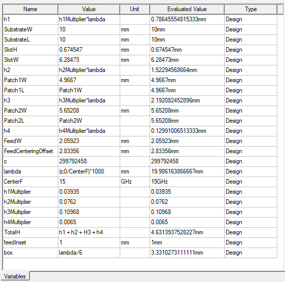
The unit cell is inherently simple in design, albeit more complicated than a simple inset fed patch antenna. There are four different substrate heights to optimize, a microstrip feed line, the slot width and thickness, the patch element dimensions, and the dielectric constants of the substrates.
| Parameter | Range |
|---|---|
| H1 | 0.041 to 0.62 \(\lambda\_0\) |
| H2 | 0.084 to 0.121 \(\lambda\_0\) |
| H3 | 0.077 to 0.176 \(\lambda\_0\) |
| H4 | 0.008 to 0.062 \(\lambda\_0\) |
| \(\epsilon\_r1\) | 1.78 to 2.62 |
| \(\epsilon\_r2\) | 2.28 to 2.77 |
| \(\epsilon\_r3\) | 1 to 1.36 |
| \(\epsilon\_r4\) | 2.05 to 4.62 |
| Feed Width | 50 \(\Omega\) |
| Lower Patch | 0.3 \(\lambda\_0\) Square |
| Upper Patch | 0.36 \(\lambda\_0\) Square |
| Slot Size | No set starting position, used wavelength-scaled solution |
| Feed Length | No set starting position, used wavelength-scaled solution |
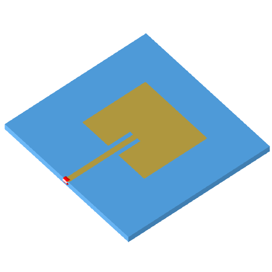
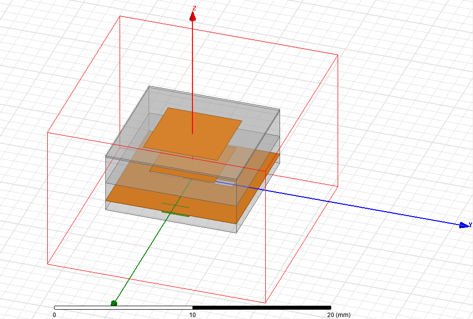
Fig. 4. shows the completed design in HFSS with these parameters
Optimized Results
To ensure repeatable, stable, and sound results, HFSS was configured to solve the mesh at the highest frequency in band (18 GHz) was a Delta-S of 0.001. In addition, a mixed-order domain decomposition analysis technique was utilized to minimize solution time and RAM usage on the host machine. Finally, a minimum of three passes with two simultaneous convergences was set to verify simulation stability.
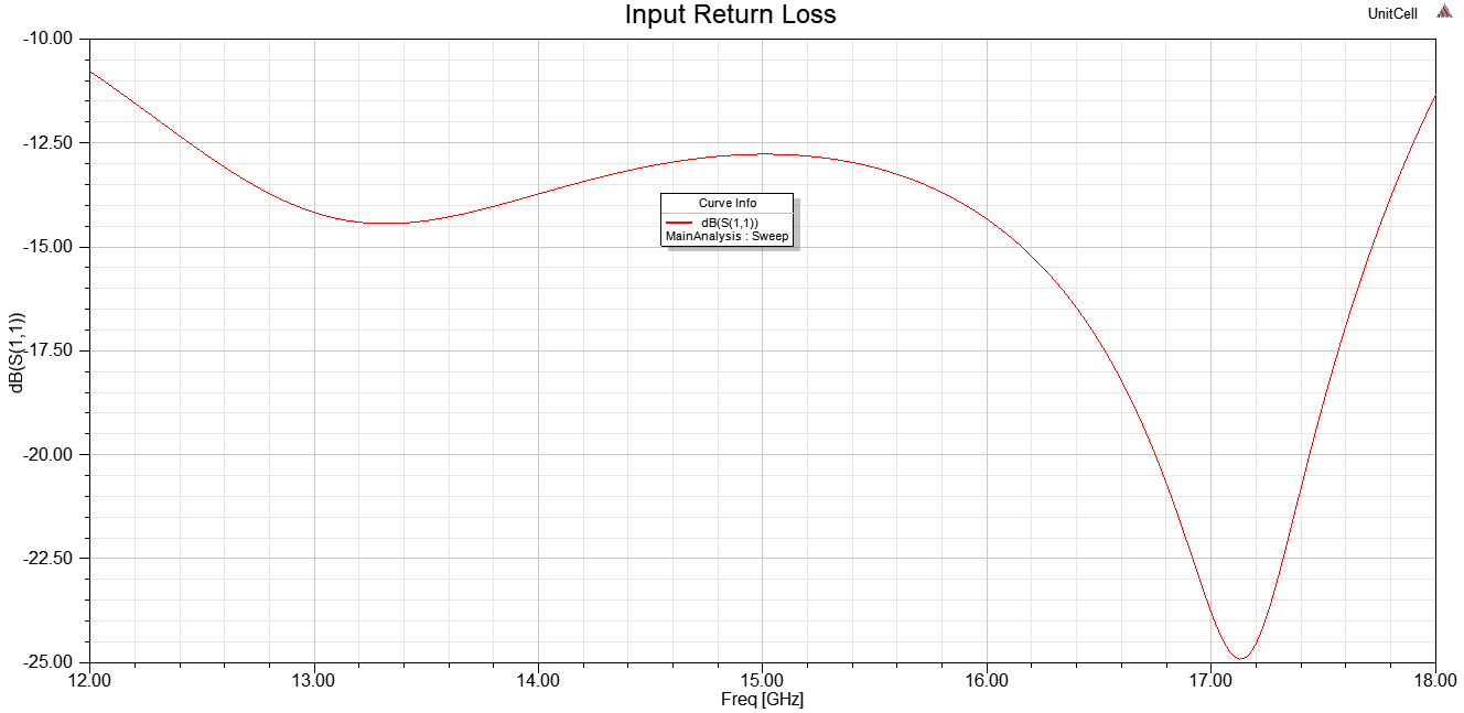
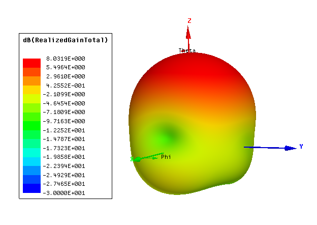
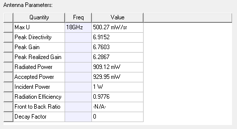
An optimization was run for five days with a very steady decrease in the cost function (S(1,1) <= 10dB in band). After over 200 iterations, the design converged. Using the solution, substrates with realizable \(\epsilon\_r\) values and thicknesses had to be found. Substituting real substrates with one dynamic layer (machineable foam), another optimization was run. Also, the lumped port was inset into the patch to alleviate strange boundary conditions resulting from edge-fed microstrip. Similarly, many iterations and many days passed before the solution converged. The final design is shown in Fig. 4. Input return loss is verified better than 10 dB in band in Fig. 5. Fig. 6. shows the unit cell radiation pattern. Efficiency of the unit cell is 97.76% with other excellent antenna parameters enumerated in Fig. 17.
Array
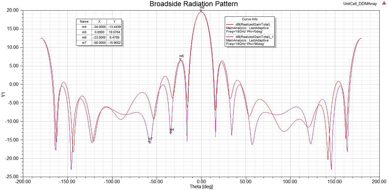
After the unit cell's input match and pattern were satisfactory, we can apply the regular array tool in HFSS to multiply this element pattern by an array factor to simulate an ideal array of this type of antenna. Fig. 7. shows the broadside performance of the array. Fig 8 shows the performance if an incremental phase shift was applied to the elements to steer the beam in either X, Y, or both.
The optimized dimensions are enumerated in Appendix II.
Full Wave Array Simulation
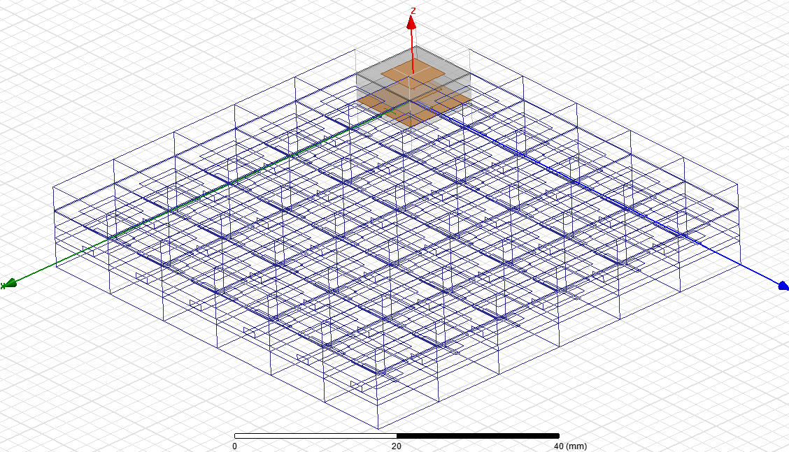
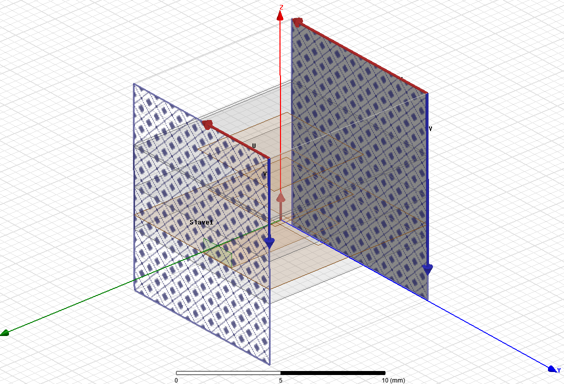
As the unit cell individually looked acceptable and the array factor performance gave enough gain to tolerate a small drop in performance, it was time to move on to the full wave simulation of the array. Normal methods for solving an array such as this involve copying and merging the unit cell elements. The problem becomes a RAM requirement, however. Because the array is electrically large, the number of mesh vertices increase exponentially. My host machine has only 16 GB of RAM, which crashed the simulation in less than 15 minutes. There is, however, a different approach to full wave finite array simulation: domain decomposition. ANSYS' own documentation was quite poor on the topic, resulting in a week's worth of effort learning the setup procedure for this simulation. The setup procedure is as follows: A unit cell has master and slave boundaries assigned on its outer-most faces. A master boundary has an assigned slave with local coordinate systems U and V. These boundaries force E field continuity as they will connect in the array setup. For the E field to be continuous across the boundary, the array must be approximated to be infinite. Because our array is not infinite, but very much finite, an outer air box is used to simulate an explicit array setup. So, as far as the solver is concerned, it needs to mesh and solve the outer edge, and only one internal unit cell with the periodic boundary. As the E field solution exists, this simulation gives full S-Parameter data as well as gain information with significantly less solution time and RAM. This solution took three days on the CIRCE cluster at USF. The complete array is shown in Fig. 12 with an example of a Master/Slave boundary pair in Fig. 13. The following analysis was performed at 18GHz, which should be the worst case for the array. Due to the time constraint, I was unable to simulate the radiated fields at the other frequencies. The unit cell had good performance at 12GHz with other 8 dB of gain, so due to the fact that we are seeing a good transition to an array, I believe it is a safe assumption that the array is working from 12 GHz given the return loss.
Gain Performance
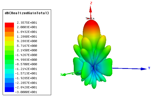
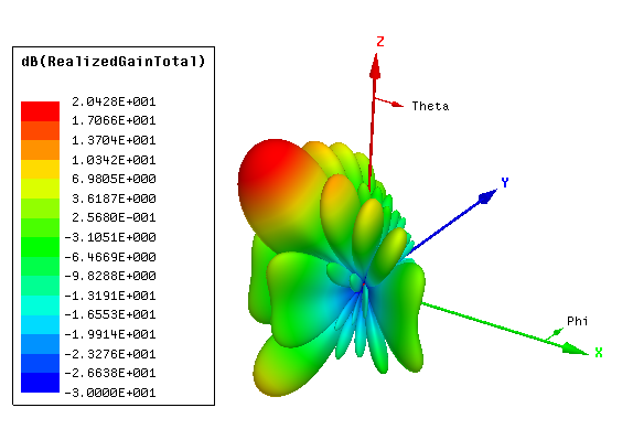
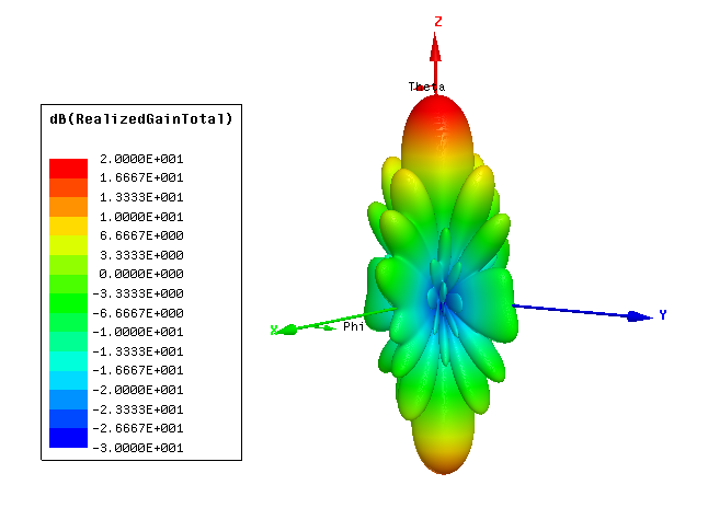
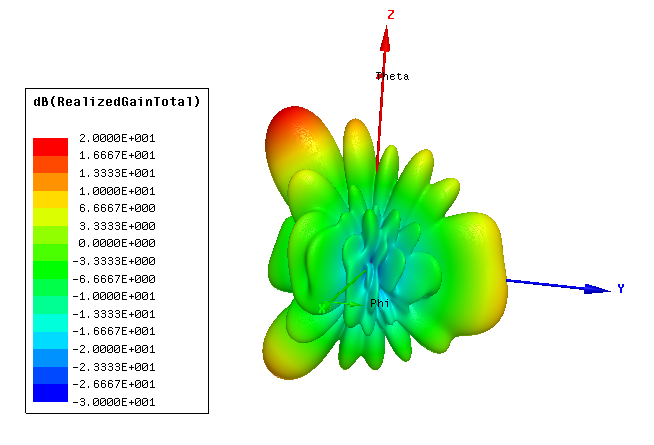
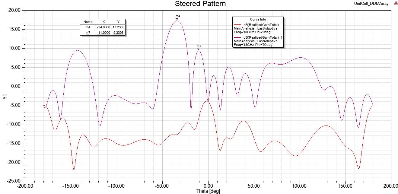
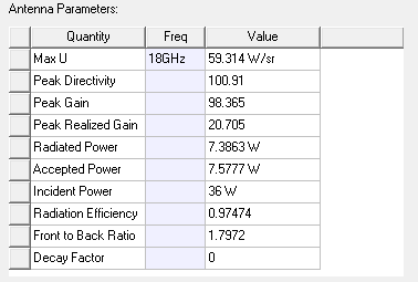
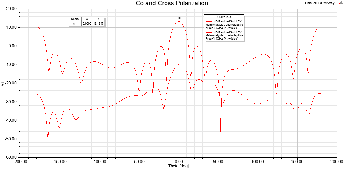
As seen in Fig. 9 and 10, the broadside pattern of the full wave has good agreement with the array-factor solution from previous analysis. A peak gain is shown to be 19.6 dB, which is due to the effect of cell coupling. In Fig. 10, it is clear to show the array in broadside has good grating lobe suppression at 17 dB. Also in broadside, the array has a good front to back ratio of 7.5 dB. Using beam steering, the 3dB point is at 34 ˆ in either direction, yielding a 68 ˆ steerable distance (Fig. 14 and 15). Of course, grating lobe performance decreases to 10dB in the fully-steered condition. Antenna parameters otherwise look quite good, with efficiency remaining at around 97% the parameters for the array can be found in Fig. 18. Co and Cross Polarization performance is found in Fig 19. I don't know how to fully interpret this information as the maximum gain in X is 13 dB versus the maximum gain overall. I believe the coupling excites the cross mode in some of the patches and the polarization starts to become circular.
Port Performance
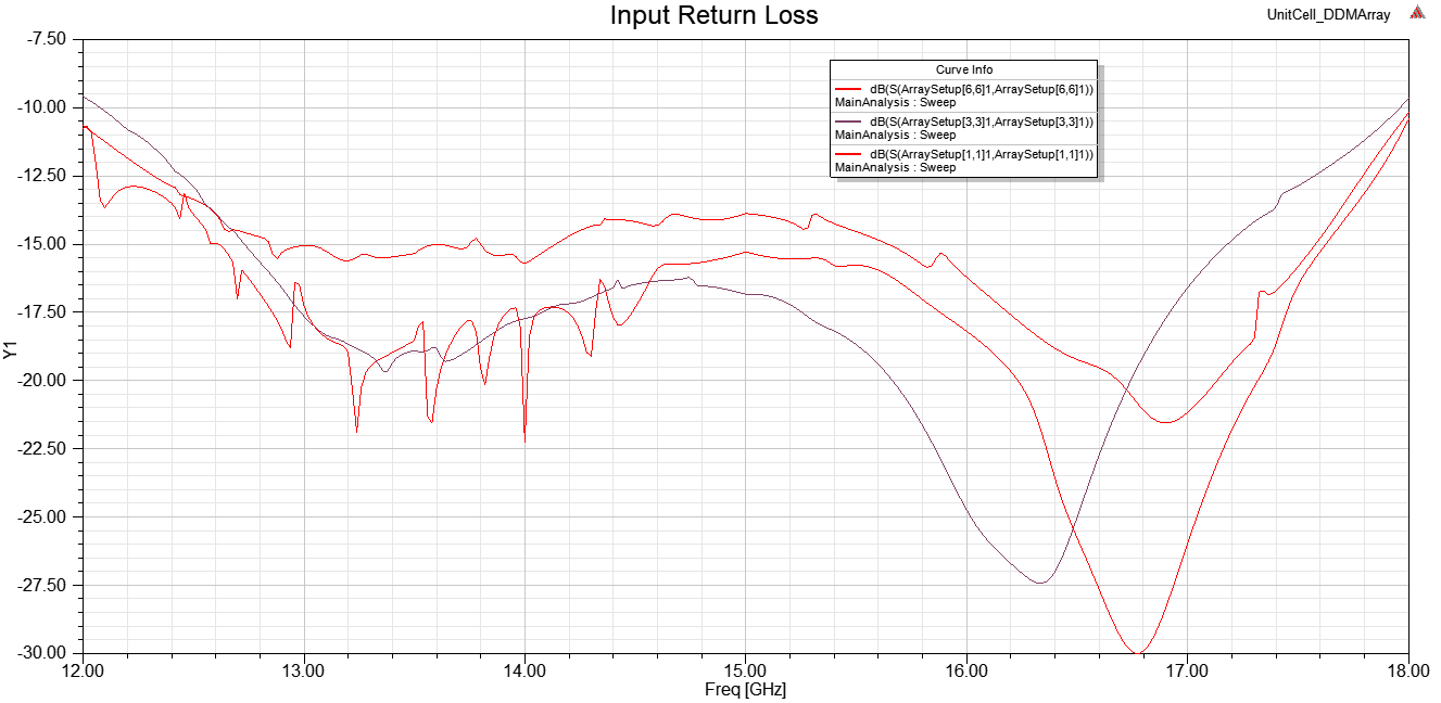
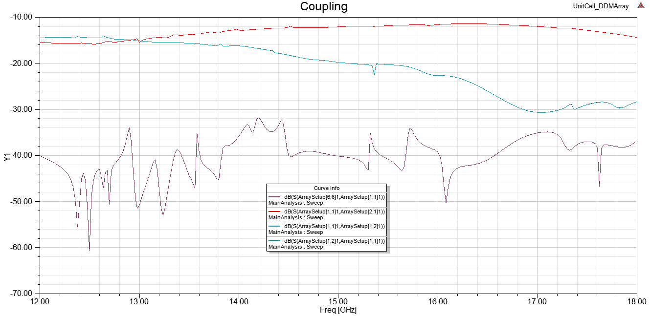
Instead of manually assigning port excitations, a MATLAB script was written to generate the source excitation list, this can be seen in Appendix I. The port performance plots didn't finishing an interpolating pass, but the displayed results are after 51 points, and show a good trend. Fig 11. shows the input return loss of a few cells. S(1,1) is the leftmost corner, the next is a cell in the center, and finally there is a cell on the opposing side. All of them show variation, but they maintain <= 10dB in the operation band. Fig. 16 displays the coupling between a few elements in the array. As is obvious, the cells close together experience a coupling factor almost 10dB. This is not very good performance. Further improvement needs to be made to reduce this coupling. Coupling between the outer elements are satisfactory.
Next Steps
Fabrication Considerations
The first step in fabrication considerations was already taken as the unit cell was designed with realizable substrates. The foam layer would need to be either hand surfaced or machined. The copper layers would be etched with photolithography onto the substrates. In fact, the main reason there even exists a layer four is because of the lack of ability to etch copper on the foam layer. Once the layers are produced, they are laminated with conventional PCB lamination methods. The hobbyist would use super glue and pressure, but a professional environment has more impedance controlled solutions. For the actual lamination procedure, alignment holes would need to be produced along the edge to accept pins. Finally, a feeding network would need to be designed. As this is a phased array, each antenna needs to be individually controlled with traditional T/R modules. Instead of inset feeding, we could use aperture coupling. This could be easily realizable with this design. Not only would this give PCB real estate for electronics, it simplifies the feeding system.
Closing Remarks
Further Optimization
If this array were to be considered for production, an optimization could be run on the array setup to minimize coupling. The main reason gain is less than what was simulated in the Array Factor setup is due to mutual coupling. A few different techniques could be applied: the array could be rectangular, minimizing the coupling in the H-Plane. Also, metamaterial absorbers could be used along the boundaries to absorb the incoming wave. To maximize forward performance, the array could be cavity backed to increase the front to back ratio.
Conclusions and Lessons Learned
In the process of developing this antenna array, I have become very familiar with the implementation of an array in HFSS. Using modern tools such as FA-DDM helped reduce the solver's workload. It wasn't without its difficulty, but it has been shown that a patch antenna array can be created that is 6 cm^2 with 20 dB broadside gain, steerable to \(62^{\circ}\), and over 40% usable bandwidth. This is a major accomplishment as an array such as this would be perfect for Ku band radar applications.
Figures
Appendix I - MATLAB Source Excitation Code {#appendix-i-matlab-source-excitation-code}
clc;
clear;

beta = 130;
PortList = readtable('PortList.csv');

for x = 1:36
    thisPhase = beta*mod(x-1,6);
    if thisPhase >= 360
        thisPhase = thisPhase-floor(thisPhase/360)*360;
    end
    PortList.Phase(x) = cellstr(thisPhase + "deg");
end

writetable(PortList,'newPortList.csv')
Appendix II - Design Variables {#appendix-ii-design-variables}